4.4 Concatenated 32-bit timer
The described type B and C timers, as already mentioned, could be concatenated to form a 32-bit timer. Functional block diagram of the concatenated 32-bit timer is shown in Fig. 4-8.

Fig. 4-8 Type C timer functional block diagram (timer 3 module)
The 32-bit timer of Fig. 4-8 is formed by combining the timer2 and timer3 modules. The timer4 and timer5 modules could be combined in a similar way. The formed 32-bit timer is a general purpose (GP) timer and could be configured by the control bits to operate in the following modes:
- 32-bit timer.
- 32-bit synchronous counter.
It is significant to note that the timer2 and timer3 modules could independently operate as 16-bit timers in the all operational modes as the timer1 module, except in the asynchronous counter mode. The same applies for timer4 and timer5 modules.
Timer2 and timer3 modules make use of other peripherals, Input capture or Output compare, in order to realize in a simple way a pulse-width modulated (PWM) signal or an A/D converter for triggering conversion at precise sampling times which is not possible with the timer4 and timer5 modules.
The concatenated 32-bit timer2/3 module has the ability to:
- A/D event trigger,
- operate in gated time accumulation mode,
- prescaler select,
- operate in IDLE state, and
- generate an interrupt request upon the concatenated counter register TMR2/TMR3 is equal with the preset register PR3/PR2.
Adjustment of the mode of operation of the concatenated timer2/3 module is performed by the control bits in T2CON and T3CON.
Attention!
If the timer2 and 3 modules operate independently, the operation modes are adjusted by T2CON and T3CON. If they operate as the concatenated timer2/3 module, then the T2CON control bits are adjusted and T3CION control bits are ignored. The timer2 module clock and gate inputs are used for the concatenated 32-bit timer2/3 module. An interrupt of the 32-bit timer is generated with the T3IF flag and the corresponding T3IE enable bit.
4.4.1 32-bit timer mode
In the 32-bit timer mode the timer is incemented at each instruction cycle until the value of the concatenated counter register TMR3/TMR2 is equal to the concatenated preset register PR3/PR2. Then the counter register is reset to ‘0’ and an interrupt request is generated with the bit T3IF.
NOTE: Synchronous reading of the 32-bit TMR3/TMR2 register is carried out by reading timer2 module 16-bit TMR2 register as the Less Significant word (LS). During reading of TMR2 register the value of the TMR3 register is transferred to the temporary register TMR3HLD. The process of the 32-bit reading is concluded by reading the value of the Most Significant word (MS) from the register TMR3HLD.
The synchronous 32-bit writing is performed in two steps inversly to the reading. At first the higher significant word is written in the TMR3HLD and then the Less significant word is written in TMR2. During the writing in the TMR2 register the vaules of TMR3HDL and the counter register TMR3 are transferred to TMR2.
The following example demonstrates how the concatenated timer2 and 3 modules can be used in a 32-bit timer.
Example:
Turn on and off a LED diode at port D approximately once every two seconds. The example uses the concatenated timer2 and 3 modules having 256 times slower clock than that of the dsPIC device. At each 100 000 clocks of timer1 interrupt routine
Timer23Int is called and the value at port D is changed.
program TestTimer23;
procedure Timer23Int; org $22; // Address in the interrupt vector table of timer3
begin
  LATD := not PORTD; // Invert port D
  IFS0 := 0; // Clear interrupt request
end;
begin
  TRISD := 0;              // Port D is output
  LATD  := $AAAA;          // Initial value at port D is set
  IPC1  := IPC1 or $1000;  // Timer3 priority is 1
  IEC0  := IEC0 or $0080;  // Timer3 interrupt enabled
  PR2   := 34464;          // Interrupt period is 100 000 clocks
  PR3   := $0001;          // Total PR3/2=1*65536 + 34464
  T2CON := $8038;          // Timer2/3 is enabled, internal clock is divided by 256
  while TRUE do            // Endless loop
    nop;
end.
How does one set timer2/3 module to the 32-bit timer mode? The corresponding iterrupt bits, i.e. interrupt priority T3IPC=1, interrupt request bit T3IF=0, and interrupt enable bit T3IE=1 are set first (in the concatenated timer2/3 module interrupts are controlled by the control bits of the timer3 module and the operation of the timer2/3 module is controlled by the control bits of the timer2 module). Then the operation of the timer is activated TON=1, 32-bit operation is selected T32=1, and in this case the prescaler is configured for 1:256 ratio TCKPS<1:0>=11. The preiod register PR2/3 contains the value 100 000 distributed according to the formula PR3/2=PR3*65536 + PR2, PR3=1 and PR2=34464.
How does one calculate the period of interrupt calls? Let the internal clock be adjusted to 10MHz. The corrsponding period is 100ns. Since the clock is divided by 256 (the prescaler reduces the clock 1:256) to form the clock of the timer, it follows that 100ns*256 = 25600ns, i.e. 25.6µs. At each 100 000 clocks an interrupt is called, i.e at each 2.56s or approximately once every two seconds.
T = 100 000*25.6µs = 2.56s.
4.4.2 32-bit synchronous counter mode
In a 32-bit synchronous counter mode the concatenated timer TMR3/TMR2 is incremented on each rising edge of the external clock signal which is synchronized with the phase of the internal clock signal of the microcontroller. When the value of the counter register TMR3/TMR2 is equal to the preset value of the PR3/PR2 register, the content of the register TMR3/TMR2 is reset to ‘0’ and an interrupt request is set by the bit T3IF.
The following example demonstrates how the timer2/3 module can be used in the 32-bit synchronous counter mode.
Example:
Use the timer2/3 for counting the external clock pulses at pin T1CK. After 10 pulses an interrupt
Timer23Int occurs and increments the value at port D. Block diagram of connecting the timer 2/3 to the external source of clock is shown in Fig. 4-9.

Fig. 4-9 Block diagram of connecting the timer 2/3 of a dsPIC30F4013 to an external source of clock
program TesTimer23;
procedure Timer23Int; org $22; //Address in the interrupt vector table of timer3
begin
  INC(LATD);                   //Increments the value of PORTD
  IFS0 := 0;                   // Clear interrupt request
end;
begin
  TRISD := 0;             //PORTD is output
  TRISC := $2000;         //PORTC<13>=1 T2CK is input pin
  LATD  := $0;            //Initial value at PORTL is set
  IPC1  := IPC1 or $1000; //Interrupt priority of timer3 is 1
  IEC0  := IEC0 or $0080; //Interrupt of timer3 enabled
  PR2   := 10;            //Interrupt peiod is 10 clocks
  PR3   := 0;             //Total PR3/2=0*65536 + 10
  T2CON := $800A;         //Timer2/3 is synchronous counter of external pulses
  while TRUE do           //Endless loop
   nop;
end.
How does one set timer 2/3 module to the synchronous counter mode? Prescaler 1:1 is selected, external clock is enabled TCS=1, 32-bit operation is enabled T32=1, the operation of the timer1 module is enabled TON=1 in the control register T2CON (in 32-bit operation the control bits T3CON are ignored), interrupt bits of timer2/3 module are set (in the concatenated timer2/3 interrupts are controlled by the control bits of timer3 module), priority of interrupts T3IPC=1, interrupt request bit T3IF=0, and interrupt enable bit T3IE=1.
4.4.3 Gated time accumulation mode
The concatenated 32-bit timer module can be used in the gated time accumulation mode.This mode allows that the TMR3/TMR2 counter is incremented by the internal clock TCY as long as the state of the external GATE signal (pin T2CK) is high. In this way one can measure the length of the external signal. In order to operate the 32-bit timer in this mode, it is required to set the control bit TGATE (T2CON<6>) to enable this mode, select the clock source TCS=0, and enable timer operation TON=1 in the control register T2CON. In this mode the timer2 module is the internal clock source. Control bits of the timer3 T3CON are ignored.
The interrupt request is generated on the falling edge of the external GATE signal or when the value of the TMR3/TMR2 counter reaches the preset value in the PR3/PR2 register.
Attention! The falling edge of the external GATE signal does not reset the TMR3/TMR2 counter; if desired, this has to be done by the user software.
Example:
Use timer 2/3 in the gate time accumulation mode. GATE signal is applied to pin T1CK. The length of the signal is measured and displayed at pord D. Block diagram of the timer2/3 connection to an external clock sourse is shown in Fig. 4-10.

Fig. 4-10 Block diagram of the timer2/3 connection to an external clock source
program TestTimer23;

procedure Timer2Int; org $20; //Address in the interrupt vector table of timer2
begin
  LATD := TMR2;               //Signal length is displayed at port D
  IFS0.6 :=0;                 //Interrupt request cleared
end;

begin
  T2CON := 0;                 //Stops the Timer2 and reset control register
  TMR2 := 0;                  //Clear contents of the timer register
  PR2 := $FFFF;               //Load the Period register with $FFFF
  IFS0.6 :=0;                 //Interrupt request cleared
  T2CON.6 := 1;               //Set up Timer2 for Gated time accumulation mode
  T2CON.15 := 1;              //Start Timer2
  TRISD := 0;                 //PORTD is output
  TRISC := $2000;             //PORTC<13>=1 is input pin
  IEC0.6 := 1;                //Timer2 interrupt enable
  while TRUE do               //Endless loop
    nop;
end.
Why the period registers PR2 and PR3 are set to the maximum value and how does one measure even longer pulses? The main reason is to measure as long pulses as possible, i.e. the interrupt does not occur because the concatenated registers TMR3/TMR2 and PR3/PR2 are equal but, if possible, it is the ceonsequence of the falling edge of the GATE signal. Measuring even longer pulses can be accomplushed by setting the prescaler to higher reduction ratios 1:8, 1:64, or 1:256. In this way the range of measurement is extended but the accuracy is reduced.

Fig. 4-11 Description of the gated time accumulation mode of the 32-bit timer2/3 module
The concatenated timer2/3 has the ability to trigger an A/D conversion. This is realized by setting the corresponding control bits in the register ADCON<7:5> (SSRC<2.0>=010). When the value of the concatenated counter register TMR3/TMR2 becomes equal to that of the PR3/PR2 register, the A/D converter is triggerred and an interrupt request is generated.
NOTE: The timer modules 2 and 3 could operate independently as 16-bit timers. They coud be configured to operate in the following modes: 16-bit timer, 16-bit synchronous counter, and 16-bit gated time accumulation. The timer modules 2 and 3 can not operate as 16-bit asynchronous counters nor as real time clock sources (RTC).
As a clock source, the timer2 and 3 modules use an external clock source or the internal clock FOSC/4 with the option of selecting the prescaler reduction ratio 1:1, 1:8, 1:64, or 1:256. The selection of the reduction ratio is achieved by the control bits TCKPS<1:0> (T2CON<5:4> and T3CON<5:4>). When the timer2 and 3 modules form the concatenated 32-bit timer module, then the prescaler reduction ratio is selected by the timer2 module and the corresponding control bits of the timer3 module are ignored. The prescaler counter is reset only if: writing in the registers TMR2 or TMR3, writing in the registers PR2 or PR3, or the microcontroller is reset. It is important to note that the prescaler counter can not be reset when the timer1 module is disabled (TON=0) since the clock of the prescaler counter is stoped. Also, writing in T2CON/T3CON does not change the contents of TMR2/TMR3.
In SLEEP mode the timer2 and 3 modules are not functional since the system clock is disabled. In IDLE mode the timer2 and 3 modules will continue operation if TSIDL bit is cleared. If this bit is set, the timer2 and 3 modules will stop until the microcontroller is waken up from IDLE mode.
The characteristics of the timer4 and 5 modules are very similar to those of the timer2 and 3 modules. If concatenated to form a 32-bit timer, they could operate in the same modes as the timer2 and 3 modules. The only difference is that the timer4 and 5 modules are not used by other peripherals Iput capture and Output compare like the timer2 and 3 modules. Also, the timer5 module has no ability like the timer3 module to trigger an A/D conversion.

Fig. 4-12a Pin diagram of dsPIC30F4013
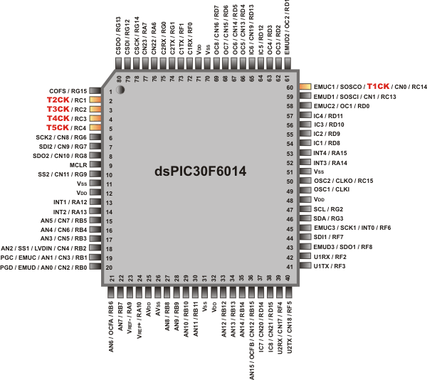
Fig. 4-12b Pin diagram of dsPIC30F6014A
Finally, a description of the registers of the timer2, 3, 4, and 5 modules of microcontroller dsPIC30F4013 is presented.
| NAME |
ADR |
15 |
14 |
13 |
12-7 |
6 |
5 |
4 |
3 |
2 |
1 |
0 |
RESET STATE |
| TMR2 |
0x0106 |
Timer2 register |
0x0000 |
| TMR3HLD |
0x0108 |
Timer3 holding register (32-bit operation only) |
0x0000 |
| TMR3 |
0x010A |
Timer3 register |
0x0000 |
| PR2 |
0x010C |
Period register 2 |
0xFFFF |
| PR3 |
0x010E |
Period register 3 |
0xFFFF |
| T2CON |
0x0110 |
TON |
- |
TSIDL |
- |
TGATE |
TCKPS1 |
TCKPS0 |
T32 |
- |
TCS |
- |
0x0000 |
| T3CON |
0x0112 |
TON |
- |
TSIDL |
- |
TGATE |
TCKPS1 |
TCKPS0 |
- |
- |
TCS |
- |
0x0000 |
Table 4-2 Description of the registers of the timer2 and 3 modules
TON – Timer on control bit (TON=1 starts the timer, TON=0 stops the timer)
TSIDL – Stop in IDLE mode bit (TSIDL=1 discontinue timer operation when device enters
        IDLE mode, TSIDL=0 continue timer operation in IDLE mode)
TGATE – Timer gated time accumulation enable bit (TCS must be set to 0 when TGATE=1)
TCKPS<1:0> - Timer input clock prescale select bits
      00 – 1:1 prescale valu
      01 – 1:8 prescale value
      10 – 1:64 precale value
      11 – 1:256 prescale value
T32 – Timer 32-bit mode of timer4 and 5 select bit (T32=1 32-bit mode selected, T32=0 timer2
      and 3 modules operate in 16-bit mode)
TCS – Timer clock source select bit
      (TCS=1 external clock from pin T1CK, TCS=0 internal clock FOSC/4)
NOTE: Reading unimplemented bits gives '0'.